Performance Rating
The Radeon R9 A375 was a mobile graphics chip by AMD, launched in 2015. Built on the 28 nm process, and based on the Venus graphics processor, in its Venus XTX variant, the chip supports DirectX 12. Even though it supports DirectX 12, the feature level is only 11_1, which can be problematic with newer DirectX 12 titles. The Venus graphics processor is an average sized chip with a die area of 123 mm² and 1,500 million transistors. It features 640 shading units, 40 texture mapping units, and 16 ROPs. AMD has paired 2,048 MB GDDR5 memory with the Radeon R9 A375, which are connected using a 128-bit memory interface. The GPU is operating at a frequency of 1015 MHz, memory is running at 1125 MHz (4.5 Gbps effective).
Contents:
Memory ML Performance Compute Power Architecture & Compatibility ML Software Support Clocks & Performance Power Consumption Rendering AdditionalMemory
Memory Size
Memory Type
Memory Bandwidth
Memory Bus Width
ML Performance
FP16 (Half Precision)
BF16 (Brain Float)
TF32 (TensorFloat)
Compute Power
FP32 (Single Precision)
FP64 (Double Precision)
CUDA Cores
RT Cores
Architecture & Compatibility
GPU Architecture
SM (Streaming Multiprocessor)
PCIe Version
ML Software Support
CUDA Version
Clocks & Performance
Base Clock
Boost Clock
Memory Clock
Power Consumption
TDP/TGP
Recommended PSU
Power Connector
Additional
Slots
Release Date
Display Outputs
Renting is cheaper than buying
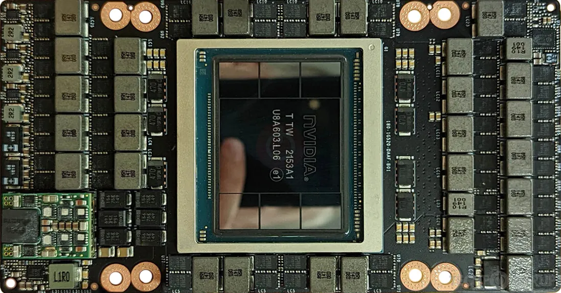
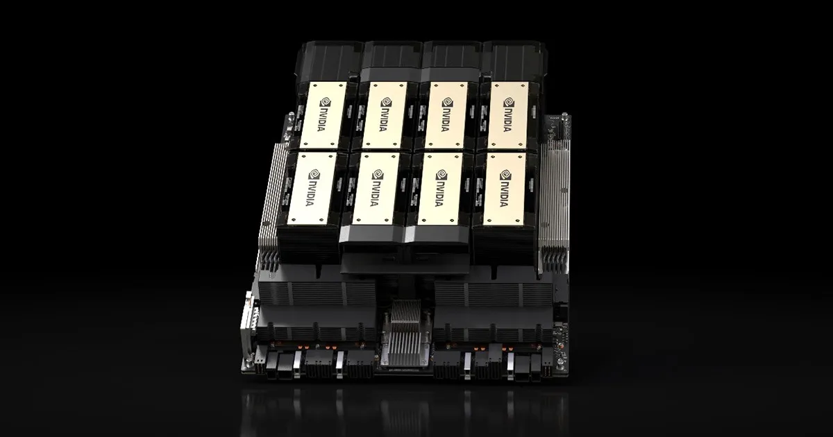
H100 80Gb SXM (80GB)
NVIDIA
Флагманская GPU на архитектуре Hopper с 80 ГБ памяти HBM3 в форм-факторе SXM. Создана для обучения и инференса больших языковых моделей, HPC задач. Поддерживает FP64, FP32, TF32, FP16, BF16, FP8 и INT8 вычисления с Tensor Cores 4-го поколения.
from 299.11 RUB/hour